|
WA1FFL Direct-Digital
VFO, Assembly Details and Instructions for Operation
Thank you for your
purchase of this kit. Here are some ideas for making the board
assembly proceed more smoothly, based on what I and others have
learned. Please read through these before beginning the assembly.
*** Important:
Before touching any integrated circuits (IC’s), make sure that
you first touch an unpainted, grounded metal object to discharge
any static electricity stored on your clothing or body.
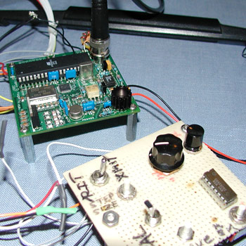
Close-Up of Control Panel with VFO
- Install
the transformer T1 first. Caution: the small “dot” on
the surface-mount transformer (T1) is pin 6. Orient
this lead on the lower-right portion of the SMT
pad for T1 and it will fit correctly. Flow a small
amount of solder on one of the corner pads for the transformer.
Then, holding down the transformer gently with pliers,
solder the corner lead and let it cool. You can now proceed
with soldering the rest of the leads, letting each one
cool as you solder it to avoid excessive heat buildup.
- In the case
of the through-hole parts, install (before soldering) all
components that have common nodes before soldering these
nodes as a group. Otherwise, solder may accidentally flow
into adjacent holes, making it difficult to route components
into these holes.
- Some of the
pads that connect to ground plane material may be more difficult
to solder to, as the ground plane tends to act as a heat
sink. If this occurs, very gently scrape the pad
a bit to remove any residual oxidation or masking material
and the solder will then flow better to the pad.
- It is highly
recommended that a low-profile, 40-pin IC socket be used
for the microprocessor U1. This will make it simple to install
software updates and improvements as they become available.
Use as high a quality socket as possible for durability
and low lead inductance. Pin 1 is in the lower right corner
of the pad. A microprocessor socket is included with the
kit.
- A good start
with the through-hole parts would be to solder the 9-volt
regulator (U4) with its heat sink installed in first,
then the regulator components (D1, F1, C1, C2, R1, and R2).
Put the heat sink (TO5 type) on first before soldering the
regulator onto the board. This is done by taking the (regulator)
metal can, inverting it, and pushing it into the heat sink
gently with long-nose pliers. Before proceeding to U5, install
D1, F1 and the +12v. supply leads and check to make sure
that the output of the 9 volt regulator is correct. Once
the second metal can regulator (U5, 3.3 volts output) is
mounted, install R3, R4, C3, and C4. Also install C37.
- Now install
the +5 volt TO-220 regulator. Be careful to orient the +5
volt regulator correctly (metal tab facing the bottom edge
of the board). The silkscreen will help you do this. You
can now check all output voltages to make sure these are
correct.
- Install the
51-ohm resistors, R6, R7, R8, R9, and R14.
- Install R5,
C10, R16, C11, C7, and C8.
- Install the
output stage components: U3, R10, R11, R12, R13, and R15.
Also install C29, C32 and C33.
- Install Y1
and U8, and the BNC output connector if you plan to use
it. If the BNC connector solder pins are too tight, try
gently “working” the mounting holes with a manual drill,
using a 1/16” size drill bit.
- When installing
the output filter, solder in C34, C35, and C36 first. These
are conventional, ceramic through-hole capacitors. Then,
install L4 and L5 on the bottom of the board.
This will help reduce crowding of components in this region.
Carefully dress leads to insure clearance of the BNC output
connector, if you choose to install it. Sufficient wire
is supplied to wind both L4 and L5.
- Solder in
U10, the 10K ohm resistor pack next to the microprocessor
(left edge of circuit board). Be sure you have the common
+5 volt pin in the correct position. There is a mark (i.e.,
a “dot”) on the resistor pack and a small “X” on the circuit
board footprint for this part that marks the + supply pin.
- Be careful
of metallic standoffs or any metallic surfaces (connector
shells, cable shields, etc.) touching the U4 or U5 regulator
cans. They are electrically “hot” (i.e., they have Vout
on them!). The LM117’s do have thermal shutdown protection,
as a matter of interest.
- The first
lowpass filter is pre-installed with the 30 MHz Chebychev
version of the circuit, and therefore C22-C24 are not used
(omitted).
- Install the
microprocessor socket and insert U1, the microprocessor,
taking care that pin 1 of the micro’ is on the lower right
corner of the socket, as the board faces you.
- Before wiring
up the display and shaft encoder, you can check the board
output.
First,
make sure the key line (microprocessor pin 23) is grounded.
Otherwise, the output will be inhibited in the (keying)
software.
With
no 50-ohm termination a clean 10 MHz sine wave of
about 1 volt peak amplitude should be present at the output.
A 50-ohm termination will reduce this by one-half (6 dB).
It will also smooth out the frequency response and should
eventually be done to terminate the output filter. Of
course, driving a 50-ohm buffer amplifier will have the
same effect.
If
you get this far, the AD9951 DDS is working and you are
in fine shape, as the display and shaft encoder work directly
off of the microprocessor and should easily come right
up.
Next,
wire up the four resistors and two capacitors for the
mechanical shaft encoder. Refer to the wiring diagram
supplied with the kit. If you mount the encoder on a panel
the 4 resistors and 2 capacitors can be wired up behind
the panel on the encoder. Shaft encoder input lines A
and B (microprocessor pins 21 and 22, respectively) and
+5v. and ground can now be connected out to the encoder
from the respective points on the VFO pc board.
The
LCD display is wired as follows: turn over the LCD
and you will see the pins numbered 1-14. Pins 1,
3, and 5 are connected to ground. Pin 2 is connected
to +5v.
Pin
4 is connected to the “RS” line on the VFO pc board (microprocessor
pin 27). Pin 6 of the LCD display is connected to “EN”
on the VFO (microprocessor pin 28). The data lines D0-D7
on the VFO board are connected to LCD pins 7-14, respectively.
Now
you can install whatever switches you will need. Minimally, you
will need a pushbutton switch connected to the “step” line (microprocessor
pin 26) so that you can adjust the tuning step sizes. RIT, CAL,
and OFFSET switches may be connected if these features are useful
to you. Otherwise, leaving these pins unconnected will cause
no problem. The SAVE, MEM (memory select) and RCL (recall) switches
will allow you to use the flash EEPROM. The 16 memory
locations increment from 0 to “F” at the bottom of the
display.
Mounting
the switches. The small push-button momentary switches
mount well on a piece of insulated perf- (perforated)
board, the kind that has small (.046”) holes spaced
0.1” apart. This material is made by Vector, among others.
The 0.1” hole spacing is meant to accommodate IC sockets
but if you mark out a square that is 0.2” (i.e., two
perf-holes) on each side, then drill holes in each corner
with a 1/8” drill, you will find that the miniature
switches fit well. Put a small bead of cement
on the bottom of the switch to fasten it to the perf-board.
You can now wire up the switches, which are normally
open but connect to ground momentarily when the button
is pushed down. The SPST switches are simple to mount
and only require one 7/32” hole apiece. Because of the
many different requirements, fabricating a control panel
is left to the operator, depending on which features
you need.
As described earlier, the software is designed to come
up at a start frequency of 10 MHz. The default step size
is 1 kHz. The carrier will have any residual error that
the clock oscillator U8 has (this can be calibrated out
later). For instance, a 50 ppm (part-per-million) clock
oscillator can generate up to a 500 Hz error at 10 MHz.
(The procedure for calibrating out this error will be
described in the next section. I performed this procedure
with a 50 ppm, 150 MHz oscillator (Connor-Winfield AC52)
driving the AD9951. After storing the calibrated carrier
into EEPROM, I reduced the error down to a few Hz after
a 15 minute warm-up). The next section (VFO Operation)
will describe how to set up calibrated sub-bands using
the flash EEPROM.
If
you need more output, I have AD8005’s in stock, and you
can duplicate the original amplifier circuit for more
gain (i.e., off-board). As the AD8005 is only rated
for about 12.6 volts across it, I would recommend a
maximum output swing of 6 volts peak-to-peak, to minimize
distortion. Try a buffer stage gain of about 15 dB. For
best results, the VFO should be mounted in a shielded enclosure.
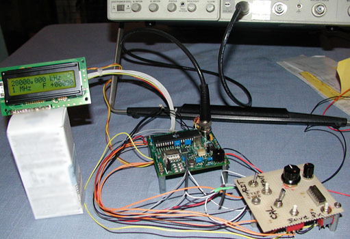
Complete VFO System
VFO
Operation
- The VFO has frequency tuning step sizes of 1 MHz down to 1 Hz. To change tuning step sizes, hold down the STEP pushbutton switch and rotate the shaft encoder until the desired step size is obtained. For best overall accuracy, use the largest practical step size available for tuning the VFO (i.e., fewest step increments to get where you are tuning to).
- The CAL function can be used to calibrate out clock error (typically 100 ppm or 50 ppm in off-the-shelf devices). Throwing the CAL switch freezes the display and adds or subtracts 1 Hz. steps to the carrier constant. The CAL function overrides the others (RIT, STEP selection) so turn the CAL switch off after calibrating the carrier. Procedure: after warming up the board for 20-30 minutes, put a frequency counter on the output. Hold down the MEM pushbutton switch and select a memory location for your configuration. There are 16 memory locations (0-9, A-F displayed on the bottom row). Turn on the CAL switch, null out the carrier error, then hit the SAVE button. The calibrated carrier will be saved in flash EEPROM, in the memory location that you have selected.
-
In this way (section 2), calibrated sub-bands can be set up (3.5 MHz, 7.0 MHz, 14 MHz, etc.) in selected memory locations. To recall a frequency configuration, hold down the MEM switch and turn the shaft encoder to the desired memory location. Let go of the MEM switch; now push the “RCL” (recall) button and the stored carrier will be loaded and displayed.
*** The VFO always comes up in Memory Location “0,” so if you want to come up right where you left off last time before power-down, select memory location “0” and hit the SAVE button before powering down. The other locations (1-F) will save whatever you have stored in them.
A Suggestion: the microprocessor is programmed for an initial start frequency of 10 MHz. If you do not have access to a frequency counter, you can still CAL out clock error by using the CAL feature and zero-beating the VFO output with the 10 MHz WWV signal on your receiver.
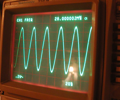
Clean Output Waveform at 28 MHz
- The RIT (receive incremental tuning) function allows the user to tune +/- 10 kHz of the displayed carrier, in 10 Hz. steps. Make sure the CAL switch is off. Throwing the RIT switch (i.e., grounding the RIT line) will enable the sub-display in the lower right hand corner of the LCD. The offset reads in Hz directly, added or subtracted to the main display. When the RIT switch is turned off, the original carrier is restored. Throwing the switch again restores the offset. If a frequency configuration is stored in memory and the RIT is enabled, the RIT offset is stored along with the configuration. Turning off the RIT switch always removes the RIT offset.
- The OFST enable line (pin 3 of the microprocessor) can be grounded to enable either a CW (700 Hz) or SSB (1.5 kHz) offset of the carrier. Grounding pin 1 of the microprocessor gives a CW offset; leaving it open will result in a SSB offset.
Custom offset frequencies are available for your own particular frequency conversion scheme; contact me for details. The offset will be added or subtracted, depending on whether pin 2 is grounded (+ offset) or left open (- offset). The OFST enable line can be tied to the key line for a keying offset, or controlled independently if the VFO is free-running.
**IMPORTANT: Use a switch debouncing filter at pins 1 and 2 of the microprocessor: place a 1 uF. capacitor to ground at pin 1, and a 100k resistor from pin 1 to +5 v. Use a separate but identical filter for pin 2. Connect the appropriate SPST switches to pins 1 and 2, and smooth, glitch-free switching of the offset mode and polarity should be the result.
VFO Switch Functions and Configuration
(i.e., I/O Control Signal Table):
(note: an open switch position is “high” because the microprocessor has internal pullup
resistors on these lines. “Low” means that you simply connect the line to ground.)
Control Signal |
High
(open) |
Low
(ground) |
Switch
Type |
| /Key |
Disable |
Enable |
Toggle or Key |
| /CAL |
CAL mode off |
CAL mode on |
Toggle |
| /Step Adjust |
|
Step Adjust |
Push Button |
| /RIT |
RIT off |
RIT on |
Toggle |
| /SAVE |
|
Save Frequency |
Push Button |
| /Memory Channel |
|
Memory Select |
Push Button |
| /Recall Channel |
|
Recall Frequency |
Push Button |
| /Offset On |
Offset Off (transmit) |
Offset On (receive) |
Toggle |
| /CW/SSB |
SSB (1.5 kHz) |
CW (700 Hz.) |
Toggle |
| /+ Offset |
(- Offset) |
(+ Offset) |
Toggle |
Filter Table, DDS-VFO Amplifier Pre-Filter
Choices
- 30 MHz Cutoff (this is actually 0.4 dB down at 30 MHz). It is a Chebyshev design and is the easiest to build by far. This filter comes pre-installed on the VFO pc board.
Omit C22-C24; L1, L2, and L3 = 330 nH.; C25,C28 = 120 pf; C26-C27 = 180 pf.
Thanks to Mitchell Lee of Linear Technology Corp. for supplying this design.
- 30 MHz Cutoff (3 dB down at 30 MHz) Elliptic Design, Supplied By Coilcraft:
C22 = 15 pf., C23 = 68 pf., C24 = 56 pf.; L1 = 330 nH., L2 and L3 = 220 nH.
C25 = 100 pf., C26 = 150 pf., C27 = 120 pf., C28 = 68 pf.
- 40 MHz Cutoff (3 dB down at 40 MHz) Elliptic
Design, Supplied by Dave Brandon of Analog
Devices (this is quite steep as evidenced by his simulation on
NuHertz design software; can be used if rolloff is less tolerable
at 30 MHz):
C22 = 56 pf., C23 = 27 pf., C24 = 10 pf.,
L1 = 160 nH., L2 = 240 nH., L3 = 270 nH
C25 = 56 pf., C26 = 120
pf., C27 = 130 pf., C28 = 82 pf.
- 60 MHz Cutoff (3 dB down at 60 MHz); you
might try this if you want to operate the VFO up at 54 MHz
in a future software upgrade (filter design supplied by Coilcraft):
C22
= 2.7 pf., C23 = 24 pf., C24 = 9.1 pf; L1, L2 = 150
nH., L3 = 120 nH.
C25 = 30 pf.,
C26 = 68 pf., C27 = 62 pf., C28 = 27 pf.
5. 160 MHz filter:
Use the values given in the QEX article.
Let me know how you make out with the VFO. I am always available for applications support at: j.hagerty@att.net.
|
|
|